![[IMAGE] Site Location](../img/case.gif)
|
Outline
ELSYCA CP-MASTER Simulation of a CP System for Buried TankELSYCA PLATINGMASTER Copper Plating of Non-uniformly Patterned Wafer Gold Wafer Plating Process in a Cupplater Decorative Cr plating process for a rack of wheels Bipolar Pulsed Simulation of a Cu Plating Process Cr Plating Process for a Rack of Shower Tap Parts Acid Zn Plating Process for a Brake CaliperDOWNLOAD Download Studies as pdf |
COPPER PLATING OF NON-UNIFORMLY PATTERNED WAFERTitle: Analysis of a copper plating process for a non-uniformly patterned wafer Bath Type: acid copper Applied software tool: Elsyca PlatingMaster Industry: Electronics Validity and Reliability: Correlation between simulated and measured layer thickness values is well above 90% Goal of Simulations: Speed up plating process, meet severe deposit uniformity specifications Description: The uniformity of electro-deposed metal layers on wafers is influenced both by the plating process conditions and the geometrical reactor configuration (current thieves, anode shape and position, screens, etc.). But in addition, a non-uniformly patterned wafer might have a huge impact on the layer thickness distribution. Figure 1 shows a wafer with complex pattern, positioned in a simple rectangular plating tank. The wafer contains free-standing Cu-line patterns with various geometries. Several line patterns with varying line widths and interline distances are arranged in four different zones (I, II, III, IV) on the wafer, as shown in figure 2. 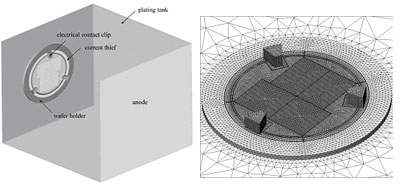
Figure 1: Plating tank configuration (left) and zoom in on the wafer with 3 contact clamps (right). 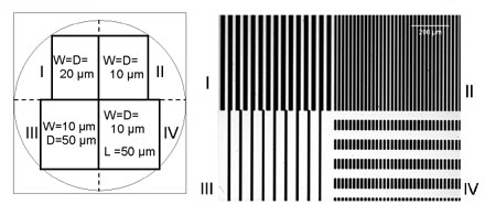
Figure 2: Geometry of different line patterns arranged on a wafer surface. Scheme showing the arrangement of the various patterns (I - IV) on the wafer and the corresponding geometries: Line width W, separation D between neighboring lines, line length L (left). Optical microscopy image from the centre of the wafer (right). The simulated current density distribution over the active wafer areas and the current thief is plotted in figure 3. The circular current thief attracts a significant part of the total current. 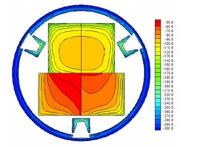
Fig. 3: Simulated current density distribution (in A/m2) over active wafer zones, contact zones and current thief. The corresponding layer thickness distribution over the active wafer zones is plotted in figure 4, together with the experimental results as obtained from X-ray fluorescence (XRF) measurements. For most spots on the active wafer zones, the accuracy of the simulated results turns out to be well above 90%. 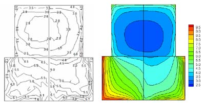
Figure 4: Simulated (left) and experimental (right) layer thickness distribution(in micron) over the active wafer zones. This example clearly illustrates that the uniformity spec's often required for wafer plating applications (i.e. standard deviations below 5 %) can simply no longer be met for non-uniformly patterned wafers, without using a highly dedicated and optimized reactor design. |
Rose Consulting Engineers LimitedWe are an independent provider of computational fluid dynamic (CFD) flow modelling services to all manufacturing sectors and are the UKs only authorised reseller/partner of Elsyca electrochemical simulation software |
|
|
|
|
|
|
|
|