![[IMAGE] Site Location](../img/case.gif)
|
Outline
ELSYCA CP-MASTER Simulation of a CP System for Buried TankELSYCA PLATINGMASTER Copper Plating of Non-uniformly Patterned Wafer Gold Wafer Plating Process in a Cupplater Decorative Cr plating process for a rack of wheels Bipolar Pulsed Simulation of a Cu Plating Process Cr Plating Process for a Rack of Shower Tap Parts Acid Zn Plating Process for a Brake CaliperDOWNLOAD Download Studies as pdf |
GOLD WAFER PLATING PROCESS IN A CUPPLATERTitle: Simulation of a gold wafer plating process in a cupplater Bath Type: Au sulphite bath Applied software tool: Elsyca PlatingMaster; Elsyca MioTraS (not commercially available) Industry: Electronics - Semiconductors Validity and Reliability: Correlation between simulated and measured layer thickness values is well above 95% Goal of Simulations: Speed up plating process, meet stringent deposit uniformity specifications, reduce costly experiments, reduce gold consumption Customer Benefits: Productivity improvements, time & cost savings, more uniform & higher quality product Description: The uniformity and quality of electrodeposited metal layers on wafers is a direct result of current density and (metal) ion concentration distributions along the wafer surface. These quantities are influenced both by the geometrical reactor configuration and the process conditions of the plating process:
A commonly used wafer plating device is the cupplater (figures 1 and 2). The wafer is positioned upside down on top of the cupplater, with the electrical contacting assured by means of several metal pins at different radial positions. The central part of the wafer is electro-active (dark blue colour in figure 1, assumed 100 % active), the outer regions (light blue) are insulating. In-between is a non-reactive photo resist area. A circular current thief (dark blue colour, 100 % active) surrounds the patterns. The outer ring is made of insulating plastic, and it is assumed that no level difference exists between the wafer and this insulating zone. Immediately below this ring, a narrow electrolyte outlet is constructed for all radial positions. The connection between the insulating cup and the outlet is made by a cylindrical neck part. The anode is perforated with a number of small holes, and acts as a diffuser for the electrolyte flow coming from the bottom inlet (figure 2, dimensions in mm, symmetry axis to the left). The inlet part below the anode, nor the diffuser holes are visualised in figure 1. For this cupplater configuration, the wafer does not rotate and the fluid flow is entirely driven by an external pump. The effect of the diffuser on the redistribution of the fluid flow from the inlet is presented in figure 3. Due to the flow acceleration, the Au2+ ion diffusion layer along the wafer surface is narrowed radially towards the outlet (figure 4). This effect is manifests entirely above the current thief in this particular case. Figure 5 shows the current density distribution along the electro-active zones of the wafer. Obviously, the current thief takes away part of the edge effects of the active wafer patterns. In order to produce a more uniform gold deposit on the wafers, two basic design features of the cupplater were improved: the neck part was enlarged, and also the flow outlet was changed. This enabled to reduce the standard deviation of the deposit thickness over the wafer with a factor 3 (from 4 % to 1.5 %) Design of the improved cell configuration was accomplished in one single effort (no experimental trial and error runs required), using the Elsyca PlatingMaster and Elsyca MioTraS software solutions. Manufacturing and assembling the improved reactor design was done in one week. Since the optimal geometrical reactor configuration and process conditions are different for each plating process (Au, Ag, Ni, Cu, ), and also for each wafer pattern and wafer size, Elsyca PlatingMaster is an invaluable tool for rapidly optimizing wafer plating processes. 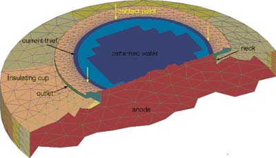
Figure 1: Cupplater configuration with patterned wafer and current thief. 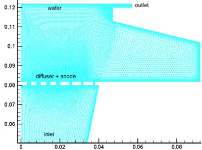
Figure 2: Vertical (axisymmetrical) cross section of the cupplater with combined diffuser/anode and inlet section. 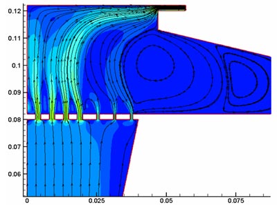
Figure 3: Fluid flow streamlines and velocity amplitude color field. 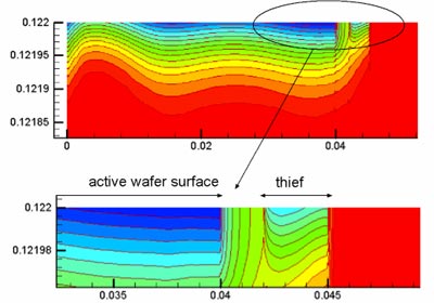
Figure 4: Au2+ concentration profiles near the wafer and current thief (X and Y axis not on scale). 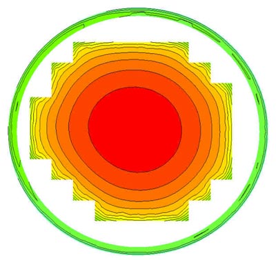
Figure 5: Current density distribution over wafer and current thief (red color corresponds to lowest current densities). |
Rose Consulting Engineers LimitedWe are an independent provider of computational fluid dynamic (CFD) flow modelling services to all manufacturing sectors and are the UKs only authorised reseller/partner of Elsyca electrochemical simulation software |
|
|
|
|
|
|
|
|