![[IMAGE] Site Location](../img/case.gif)
|
Outline
ELSYCA CP-MASTER Simulation of a CP System for Buried TankELSYCA PLATINGMASTER Copper Plating of Non-uniformly Patterned Wafer Gold Wafer Plating Process in a Cupplater Decorative Cr plating process for a rack of wheels Bipolar Pulsed Simulation of a Cu Plating Process Cr Plating Process for a Rack of Shower Tap Parts Acid Zn Plating Process for a Brake CaliperDOWNLOAD Download Studies as pdf |
BIPOLAR PULSED SIMULATION OF A CU PLATING PROCESSTitle: Bipolar pulsed simulation of a Cu plating process for printed circuit boards Bath Type: Sulphuric acid Cu Applied software tool: Elsyca PlatingMaster Industry: Electronics - Printed Circuit Boards Validity and Reliability: Correlation between simulated and measured layer thickness values is well above 90% Goal of Simulations: Determine optimal set of electrical process parameters through simulations Customer Benefits: Productivity improvements, time & cost savings, more uniform & higher quality product, accurate quoting of jobs Description: The copper plating process is one of the most critical steps in the PCB manufacturing process. Although a non-uniform copper deposition inside through- holes, micro-vias and blind holes is determining the yield, also the layer thickness distribution over the entire PCB is highly critical, in particular for multilayer designs. Bipolar pulsed current rectifiers are widely used in the high-end PCB market to reduce fall-out by more uniform deposits in blind and through-holes and on the external layers of the PCB layout.Decorative Cr plating processes produce highly non-uniform current density and layer thickness distributions. Rack design by trial-and-error will often require huge labour costs, mainly due to the large number of adjustable configuration parameters: number of parts in the rack, orientation and position of the parts, shape, dimension and position of screens and/or current thieves, etc. An entire trial and error run (rack design - rack manufacturing - plating - measuring layer thickness distributions on some parts in the rack) might take easily one week or longer. In contrast, defining the rack configuration from figure 1 in the SolidWorks CAD environment takes only a few hours, with another 1 or 2 hours to compute the resulting layer thickness distribution (figure 2) with Elsyca PlatingMaster. Hence, using Elsyca PlatingMaster will dramatically reduce the number of experimental trial and error runs, saving precious money and time. A distinction can be made between plating tank scale simulations (= macro-scale, figure 1), PCB/pattern scale simulations (= meso-scale, figure 2) and feature scale simulations (= micro-scale). Macro-scale simulations predict the difference in layer thickness from one board to another or from one printed circuit to another printed circuit on the same board. An example of the macro-scale current density distribution is given in figure 3, for normal operating conditions (left) and for another situation with 2 empty anode baskets (right). Remark that the influence of the circuit layout has not been taken into account. Meso-scale simulations however should incorporate the printed circuit layout, since the layout is determining the current and layer thickness distribution on the board. An example of a computed layer thickness distribution of the PCB pattern layout as shown in figure 2 is given in figure 4. Defining the PCB rack configuration as depicted in figure 1 in Elsyca PlatingMaster is really easy and fast (less than 30 minutes) as is computing the resulting current density distribution (figure 3). A meso-scale simulation of the pattern layout (figure 2) for a bipolar pulsed current signal (with well defined duty cycle, anodic and cathodic pulse amplitude) takes only a few minutes. Elsyca PlatingMaster can be used to optimize plating configuration issues:
In most production environments, the plating configuration is rather fixed, hence adding current thieves and background grids to the circuit layout might not always be practical. However, the electrical process parameters can be adjusted for each PCB series: for DC processes, the total current can be modified; and for bipolar pulsed current signals, the duty cycle, anodic and cathodic current pulse amplitude can be easily determined using the Elsyca software solutions. 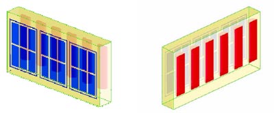
Figure 1: Vertical plating tank configuration with anode baskets (red) and PCB's (blue). 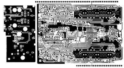
Figure 2: Typical PCB layout. 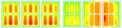
Figure 3: Current density distribution over the PCB surfaces (red corresponds to lowest current densities. Normal operating conditions (left) and situation with two anode baskets empty (right). 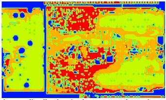
Figure 4: Layer thickness distribution (red corresponds to elevated values) over the PCB. |
Rose Consulting Engineers LimitedWe are an independent provider of computational fluid dynamic (CFD) flow modelling services to all manufacturing sectors and are the UKs only authorised reseller/partner of Elsyca electrochemical simulation software |
|
|
|
|
|
|
|
|