![[IMAGE] Site Location](../img/case.gif)
|
Outline
ELSYCA CP-MASTER Simulation of a CP System for Buried TankELSYCA PLATINGMASTER Copper Plating of Non-uniformly Patterned Wafer Gold Wafer Plating Process in a Cupplater Decorative Cr plating process for a rack of wheels Bipolar Pulsed Simulation of a Cu Plating Process Cr Plating Process for a Rack of Shower Tap Parts Acid Zn Plating Process for a Brake CaliperDOWNLOAD Download Studies as pdf |
Cr PLATING PROCESS FOR A RACK OF SHOWER TAP PARTSTitle: Simulation of a decorative Cr plating process for a rack of shower tap parts Bath Type: Decorative chromic acid, Cr (VI) Applied software tool: Elsyca PlatingMaster Industry: Appliances Validity and Reliability: Correlation between simulated and measured layer thickness values is well above 80% Goal of Simulations: Productivity improvements, time & cost savings Customer Benefits: Productivity improvements, time & cost savings, more uniform & higher quality product, accurate quoting of jobs Description: Decorative Cr plating processes produce highly non-uniform current density and layer thickness distributions. Rack design by trial and error will often require huge labour costs, mainly due to the large number of adjustable configuration parameters: number of parts in the rack, orientation and position of the parts, shape, dimension and position of screens and/or current thieves, etc. An entire trial and error run (rack design - rack manufacturing - plating - measuring layer thickness distributions on some parts in the rack) might take easily one week or longer. In contrast, defining the rack configuration from figure 1 in the Elsyca PlatingMaster/SolidWorks CAD environment takes only a few hours, with another 1 or 2 hours to compute the resulting layer thickness distribution (figure 2). Hence, using Elsyca PlatingMaster will dramatically reduce the number of experimental trial and error runs, saving valuable money and time.The copper plating process is one of the most critical steps in the PCB manufacturing process. Although a non-uniform copper deposition inside through- holes, micro-vias and blind holes is determining the yield, also the layer thickness distribution over the entire PCB is highly critical, in particular for multilayer designs. Bipolar pulsed current rectifiers are widely used in the high-end PCB market to reduce fall-out by more uniform deposits in blind and through-holes and on the external layers of the PCB layout.Decorative Cr plating processes produce highly non-uniform current density and layer thickness distributions. Rack design by trial-and-error will often require huge labour costs, mainly due to the large number of adjustable configuration parameters: number of parts in the rack, orientation and position of the parts, shape, dimension and position of screens and/or current thieves, etc. An entire trial and error run (rack design - rack manufacturing - plating - measuring layer thickness distributions on some parts in the rack) might take easily one week or longer. In contrast, defining the rack configuration from figure 1 in the SolidWorks CAD environment takes only a few hours, with another 1 or 2 hours to compute the resulting layer thickness distribution (figure 2) with Elsyca PlatingMaster. Hence, using Elsyca PlatingMaster will dramatically reduce the number of experimental trial and error runs, saving precious money and time. 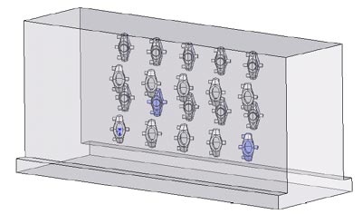
Figure 1: Rack configuration with load of 20 parts and surrounding plating tank walls; top surface represents the electrolyte level, front and back surface represent anodes. 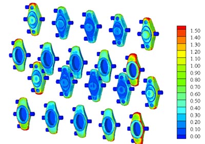
Figure 2: Layer thickness distribution (in micron) over all parts in the rack. |
Rose Consulting Engineers LimitedWe are an independent provider of computational fluid dynamic (CFD) flow modelling services to all manufacturing sectors and are the UKs only authorised reseller/partner of Elsyca electrochemical simulation software |
|
|
|
|
|
|
|
|